A.C.

AlexandreChícharo

Interdisciplinary Scientist · Inventor · Entrepreneur

I turn physical principles into sensing technologies, from a structure a few hundred nanometres across to an instrument that returns a number someone can act on.

Berlin, working across Europe

PhD Biomedical Engineering, Instituto Superior Técnico

14+ years of cleanroom and device work

Portrait of Alexandre Chícharo, arms folded, against a plain grey wall.

The most useful ideas often emerge between and across disciplines. My work is about understanding fields deeply enough to connect them — and turn those connections into technologies that matter.

Scientist
14+ years of cleanroom and device development across microfluidics, biosensing, photonics, terahertz technologies and plasmonics. My research connects physical principles, materials and experimental methods to develop new ways of measuring and understanding the world. I have published in international peer-reviewed journals and contribute to scientific peer review.
Inventor
I develop new device architectures, fabrication approaches and sensing technologies — from the first physical concept to experimentally demonstrated prototypes. My intellectual property includes a granted European patent relating to an electromagnetic-radiation polarizer (EP4024098B1) and a pending patent application relating to nanostructured SERS substrates.
Entrepreneur
Founder of nanoSpec Technologies, developing advanced molecular sensing technologies and an AI-enabled scientific intelligence platform. I work to translate scientific capabilities into practical tools, useful products and new opportunities for industry and research.

From nanodisks to nanostars.

Nanofabrication means creating and controlling extremely small structures — almost like sculpting materials at the nanoscale. Structures this small interact with light, molecules and other physical fields in ways bulk material does not, and those interactions can become new sensing technologies.

In earlier work I made gold nanodisk arrays whose placement was precise. Their Raman enhancement, however, was insufficient. Instead of returning to lithography, I asked whether those precisely positioned nanodisks could be chemically grown into plasmonic nanostars.

Plasmonics is the study of how light couples to electrons at a metal surface; at sharp tips, light concentrates into a tiny, intense field. That concentration is the basis of SERS — surface-enhanced Raman scattering — which amplifies the faint optical fingerprint of molecules sitting near the metal enough to measure them.

The technical detail

I combined top-down electron-beam patterning with controlled bottom-up gold growth, producing individual nanostars, merged architectures and spike-decorated nanoholes. In simulation, the local field magnitude at the tips was roughly three orders above the equivalent nanodisk. Experimentally, I demonstrated signal detection down to 10−14 molar for 1-naphthalenethiol.

Precision-engineered plasmonic nanostar arrays · Advanced Optical Materials, 2025 · doi 10.1002/adom.202501275
Gold nanostars at 150 000×, tilted 30°. The white bar at the lower left is 200 nm, so this frame is about 1.4 micrometres wide — a human hair is roughly fifty times wider.
Scanning electron micrograph of gold nanostars at high magnification, their spikes clearly resolved.

Gold nanostars at 150 000×, tilted 30°. The white bar at the lower left is 200 nm, so this frame is about 1.4 micrometres wide — a human hair is roughly fifty times wider.

Nanostar-pillars at 750 000×. 200 nm bar. The sharp tips are where light concentrates.
High-magnification electron micrograph of nanostar-pillars, their spikes overlapping.

Nanostar-pillars at 750 000×. 200 nm bar. The sharp tips are where light concentrates.

Dried cancer cells on a nanopillar substrate, the protrusions reaching across the array. 2 µm bar.
Electron micrograph of a dried cancer cell on a nanopillar substrate, its protrusions following the array.

Dried cancer cells on a nanopillar substrate, the protrusions reaching across the array. 2 µm bar.

A nanostar-pillar array after laser exposure: the structures melted. The failures get photographed too. 2 µm bar. Unpublished.
Electron micrograph of a nanostar-pillar array with a melted central region.

A nanostar-pillar array after laser exposure: the structures melted. The failures get photographed too. 2 µm bar. Unpublished.

How to read these images

These are electron microscope images of structures far smaller than a human hair. The scale bars show their actual dimensions. Select any image to see it larger, with its caption.

Selected publications, and the technologies behind them.

2025Precision-engineered plasmonic nanostar arraysAdv. Optical Materialssignal detection down to 10⁻¹⁴ M
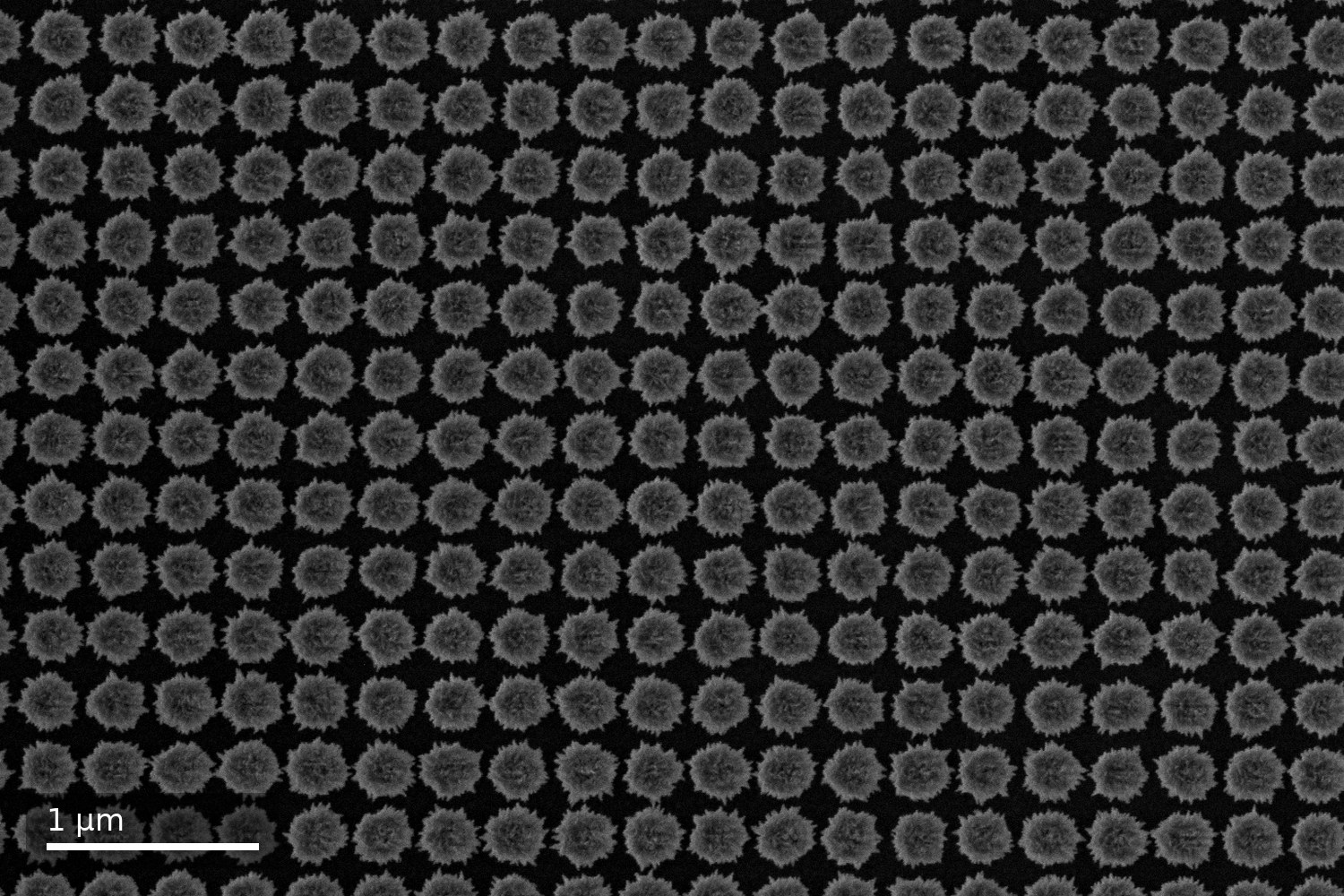
Gold nanostars on a patterned nanodisk template. 20 000×, 1 µm bar.
Ordered array of gold nanostars.

Gold nanostars on a patterned nanodisk template. 20 000×, 1 µm bar.

2025Ultra-transparent flexible terahertz polarizerOptics Express0.1 to 25 THz
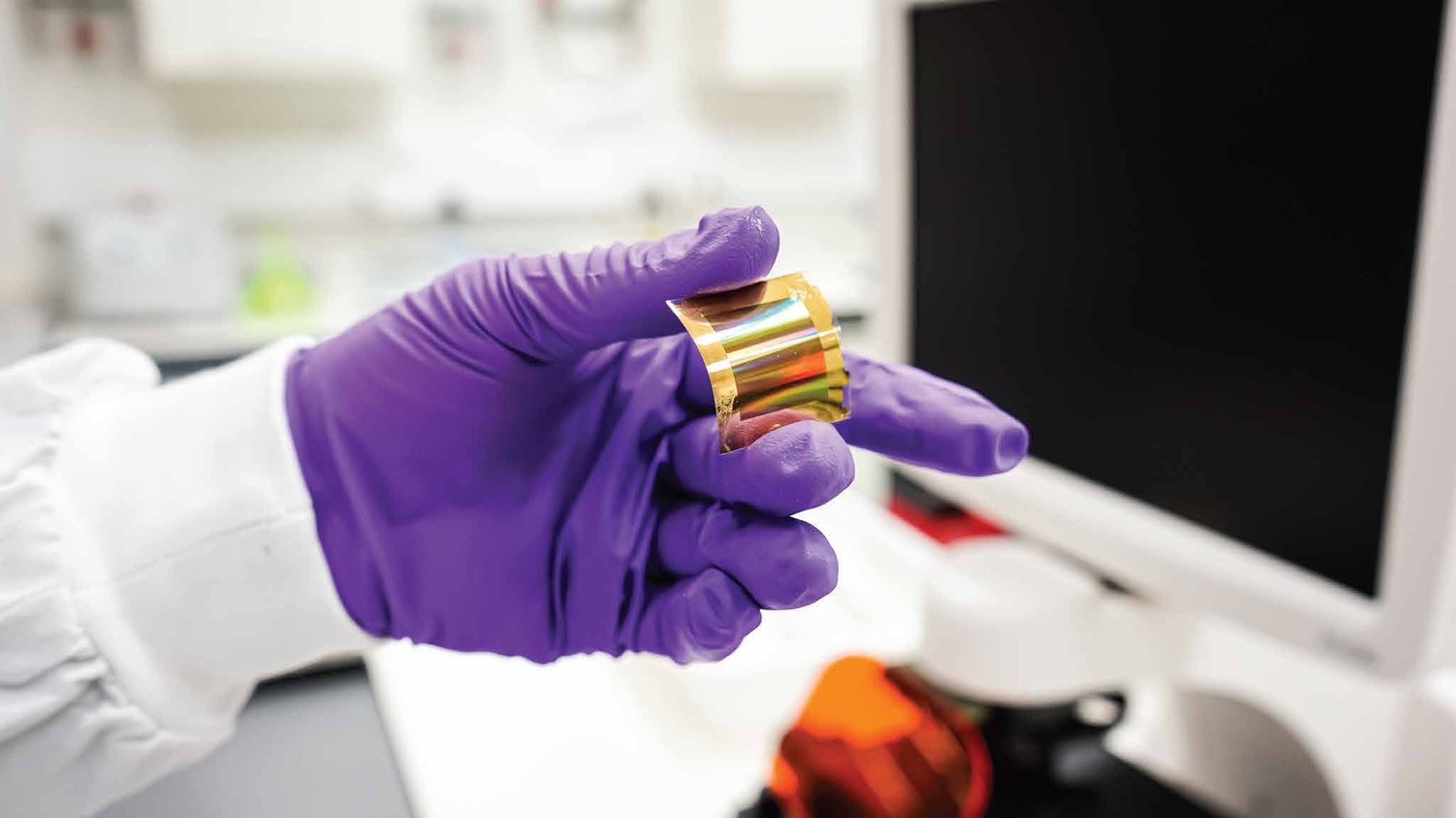
A finished polarizer: 1 µm double wire grid on a flexible transparent polymer, 0.1 to 25 THz.
A gloved hand holding a flexible gold terahertz polarizer on a transparent polymer film.

A finished polarizer: 1 µm double wire grid on a flexible transparent polymer, 0.1 to 25 THz.

2022Multiplex SERS phenotyping of single cancer cellsAdv. Optical MaterialsBIOCELLPHE
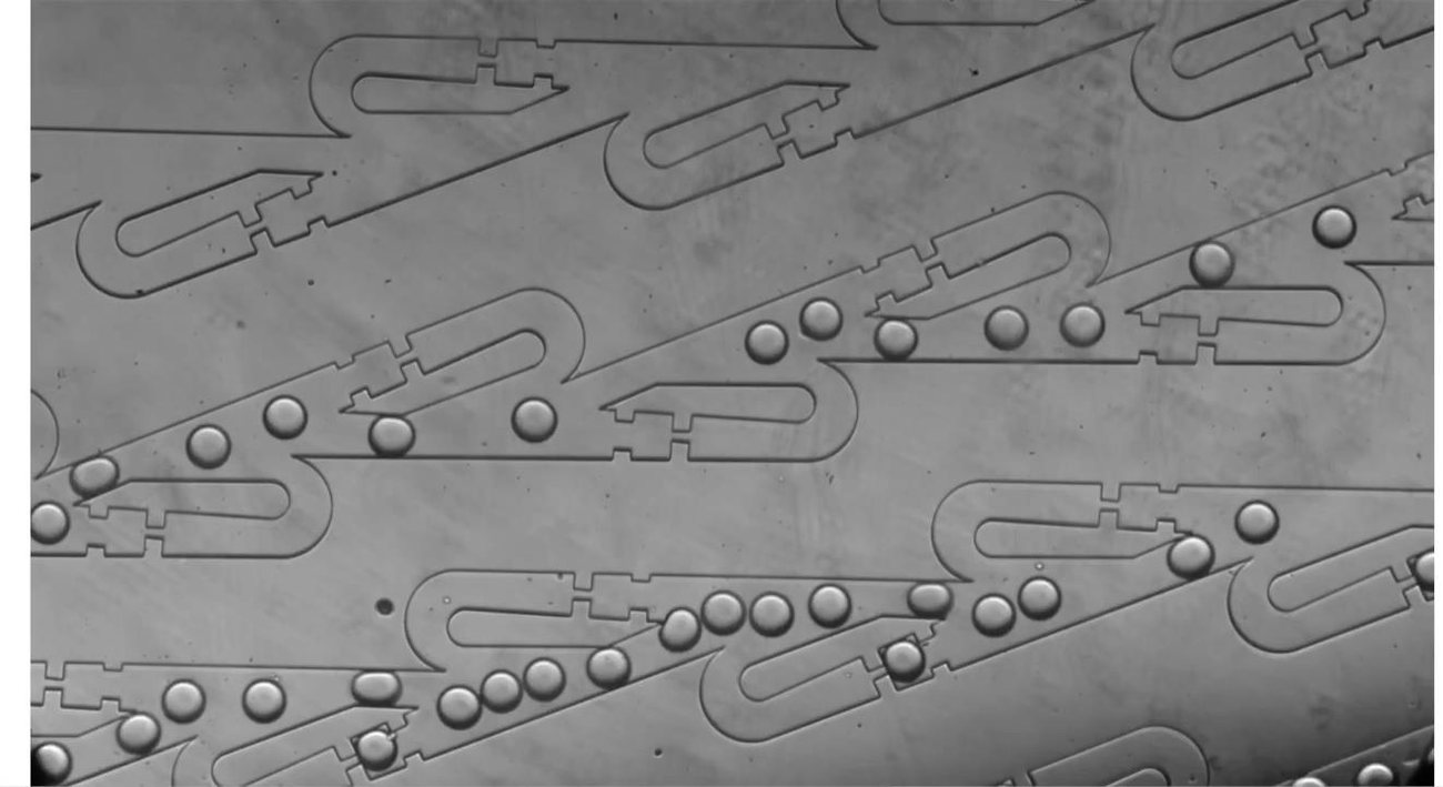
Droplets in a microfluidic channel, optical micrograph. Microfluidics is the plumbing of the very small: channels thinner than a hair that move exact amounts of liquid.
Droplets in a microfluidic channel, optical micrograph.

Droplets in a microfluidic channel, optical micrograph. Microfluidics is the plumbing of the very small: channels thinner than a hair that move exact amounts of liquid.

2020Cleanroom processes for graphene biosensorsMaterialsfar-infrared plasmonics
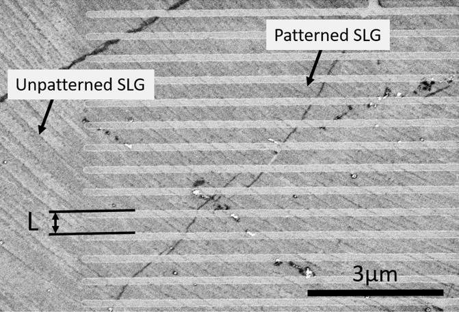
Patterned and unpatterned single-layer graphene, 3 µm bar.
Electron micrograph of patterned and unpatterned single-layer graphene.

Patterned and unpatterned single-layer graphene, 3 µm bar.

2018Magnetic microcytometer with 3D flow focusingLab on a Chipcirculating tumour cells
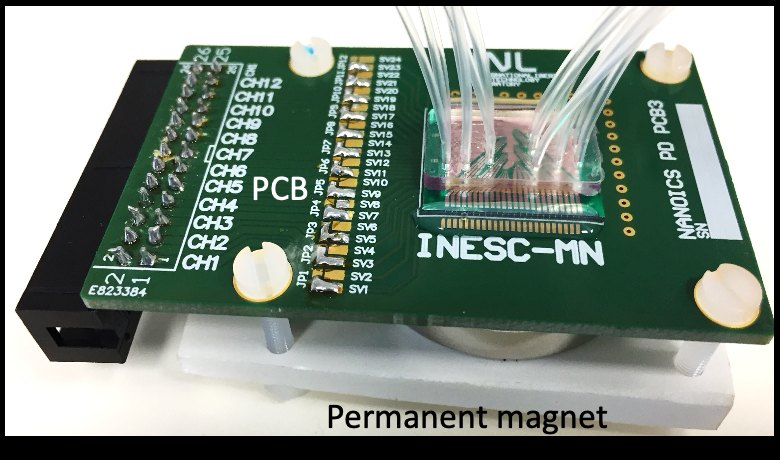
Sensor die on its carrier board over a permanent magnet, fluidic lines attached.
Sensor die on a carrier board with fluidic lines attached, over a permanent magnet.

Sensor die on its carrier board over a permanent magnet, fluidic lines attached.

2015Spintronic lateral-flow readerIEEE Trans. Magneticspoint of care
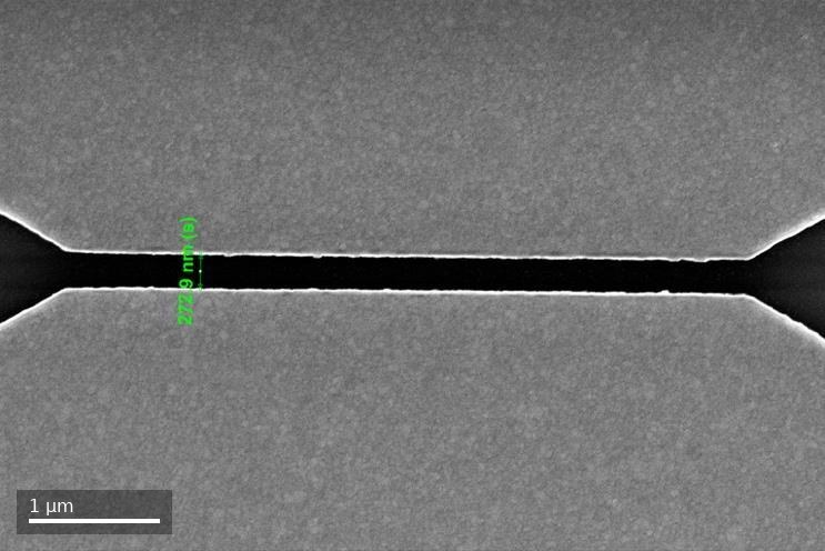
Spin valve sensor constriction. 20 000×, 1 µm bar.
Electron micrograph of a spin valve sensor constriction.

Spin valve sensor constriction. 20 000×, 1 µm bar.

Ordered array of gold nanostars.
Gold nanostars on a patterned nanodisk template. 20 000×, 1 µm bar.

Funded work, and the role I held in it.

SIREN · MSCA
Surface-enhanced Raman scattering in liquid biopsy for breast cancer. Marie Skłodowska-Curie postdoctoral fellowship at Humboldt-Universität zu Berlin, HORIZON-MSCA-2022-PF-01, grant 101109728. Fellow and principal investigator, 2023 to 2025.
TARGET
Terahertz sources using a graphene field-effect transistor. FCT–UT Austin Portugal exploratory programme. Principal investigator on the INL side, with Prof. Daniel Wasserman at UT Austin.
BEACON · canSERV
Biomarker exploration for advanced cancer detection and personalised treatment in breast cancer. Horizon Europe through canSERV, grant 101058620. Principal investigator on the access project.
FUSION
Functional nanostar array substrate for a new class of SERS biosensors. EUREKA–INL internal programme. Principal investigator.
BIOCELLPHE
Ultrasensitive biosensing platform for multiplex cellular protein phenotyping at single-cell level. H2020 FETOPEN. Research fellow and technology contributor at INL.
ACCENT Plus
Through ACCENT Plus and earlier programmes I have had access to European nanofabrication services, and I have worked with cleanrooms in Lisbon, Braga, Cork and Berlin.

Across these and earlier programmes I have attracted or co-attracted roughly €532,000 in competitive funding. Figures, identifiers and roles are documented and available on request.
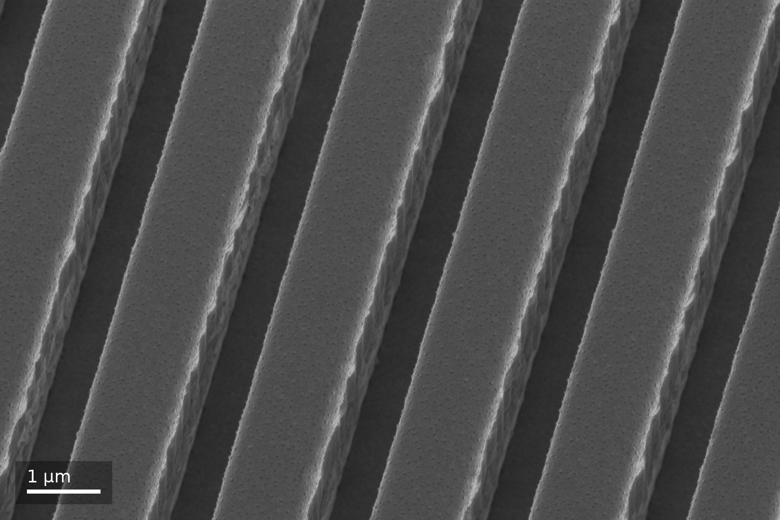
Electron micrograph of the wire grid of a terahertz polarizer, running diagonally across the frame.

I make the things I design.

Lithography, deposition, wet chemistry, functionalisation, the fluidics and the electronics around them. The designs that survive are the ones you have had to fabricate yourself, twice.

2013 – 2015

Spintronic point-of-care reader

Problem. Lateral-flow tests are cheap and everywhere, but they only answer yes or no.

Contribution. Designed and microfabricated the magnetoresistive sensor that reads them quantitatively.

Publication ↗
Spin valve sensor constriction. 20 000×, 1 µm bar.
Electron micrograph of a spin valve sensor constriction.

Spin valve sensor constriction. 20 000×, 1 µm bar.

2016 – 2018

Magnetic microcytometer

Problem. Circulating tumour cells are vanishingly rare in a blood sample and hard to isolate.

Contribution. Built the three-dimensional flow-focusing microfluidics and the integrated spin-valve sensors that count them.

Publication ↗
Sensor die on its carrier board over a permanent magnet, fluidic lines attached.
Sensor die on a carrier board with fluidic lines attached, over a permanent magnet.

Sensor die on its carrier board over a permanent magnet, fluidic lines attached.

2019 – 2021

Graphene terahertz devices

Problem. Terahertz optics — light between microwaves and infrared — lacks tunable, transparent components.

Contribution. Developed cleanroom processes for single-layer graphene devices, from biosensors to field-effect emitters.

Publication ↗
Patterned and unpatterned single-layer graphene, 3 µm bar.
Electron micrograph of patterned and unpatterned single-layer graphene.

Patterned and unpatterned single-layer graphene, 3 µm bar.

2020 – 2025

Flexible terahertz polarizer

Problem. Terahertz polarizers are rigid, narrowband or lossy.

Contribution. Invented a fabrication route for a 1 µm double wire grid on flexible transparent polymer, working from 0.1 to 25 THz. Granted European patent EP4024098B1.

Publication ↗
A finished polarizer: 1 µm double wire grid on a flexible transparent polymer, 0.1 to 25 THz.
A gloved hand holding a flexible gold terahertz polarizer on a transparent polymer film.

A finished polarizer: 1 µm double wire grid on a flexible transparent polymer, 0.1 to 25 THz.

2022 – 2025

Plasmonic nanostar SERS substrates

Problem. SERS substrates are either reproducible or strongly enhancing, rarely both.

Contribution. Combined electron-beam patterning with controlled gold growth to place sharp-tipped nanostars exactly where the light concentrates.

Publication ↗
A patterned plasmonic substrate. Each coloured bar is an array of gold nanostructures; the colour is how that array scatters light.
Tweezers holding a dark chip patterned with four plasmonic arrays glowing gold, blue and orange.

A patterned plasmonic substrate. Each coloured bar is an array of gold nanostructures; the colour is how that array scatters light.

Behind every structure on this page there is a bench, a column of parameters that had to be wrong several times first, and a measurement that either shows the peaks or does not.

A finished gold-coated sensing substrate in its carrier. Most of the work on this page fits in a box this size.
Alexandre Chícharo holding a small gold-coated sensing substrate in its clear plastic carrier box.

A finished gold-coated sensing substrate in its carrier. Most of the work on this page fits in a box this size.

nanoSpec Technologies is where this work becomes a product.

The venture
Founder of nanoSpec Technologies, a deep-tech venture developing advanced molecular sensing technologies and an AI-enabled scientific intelligence platform, for healthcare, environmental monitoring and advanced materials analysis. nanoSpec has its own site and its own story; this one is about the fourteen years of work underneath it.
nanoSpec Technologies ↗
A gold substrate under the objective with a droplet of sample on it, during a Raman measurement.
A microscope objective positioned over a gold-coated chip holding a droplet of sample.

A gold substrate under the objective with a droplet of sample on it, during a Raman measurement.

Four ways to work with me.

R&D consulting and technical advisory
Scientific and technical expertise for teams building sensing technologies: transduction choice, device architecture, nanofabrication routes and an honest read on feasibility. I work alongside your team and the facilities you already use.
Research proposals and funding
Scientific lead, co-writer or work-package contributor on European and national proposals, including Horizon Europe, EIC and MSCA instruments.
Workshops and invited talks
Technical workshops on SERS substrates, nanofabrication and biosensor design, and talks for mixed scientific audiences.
Scientific collaboration and co-development
Joint development, co-invention and advisory work with research groups and companies, including teams building an IP position.

Dive deep.Ripple wide.

Tell me what you are building and where it is stuck. If it is a fit, we start with a conversation.